fpx: easy USB‑C power for all your devices
TL;DR tiny and easy to use USB-C module to power everything; configure it anywhere, even on your phone!
My first attempt in using USB-C adapters as a power source was met with great enthusiasm. It was just a breakout board for STUSB4500 autonomous USB-PD sink controller. It has since been picked up by Sparkfun with a much better design (as you would expect).
Although sufficient, I wasn’t very happy with how much effort was needed to program the chip. It required talking I2C which for me meant an Arduino had to be available, connected to a computer with USB and a whole bunch of jumper wires. I have since used Adafruit’s MCP2221A breakout board and a Raspberry Pi but the process still has a lot of friction. So, I set out to simplify the programming aspect of STUSB4500 and this post will take you through to what became fpx, a smaller and easily configurable version of fabpide2.
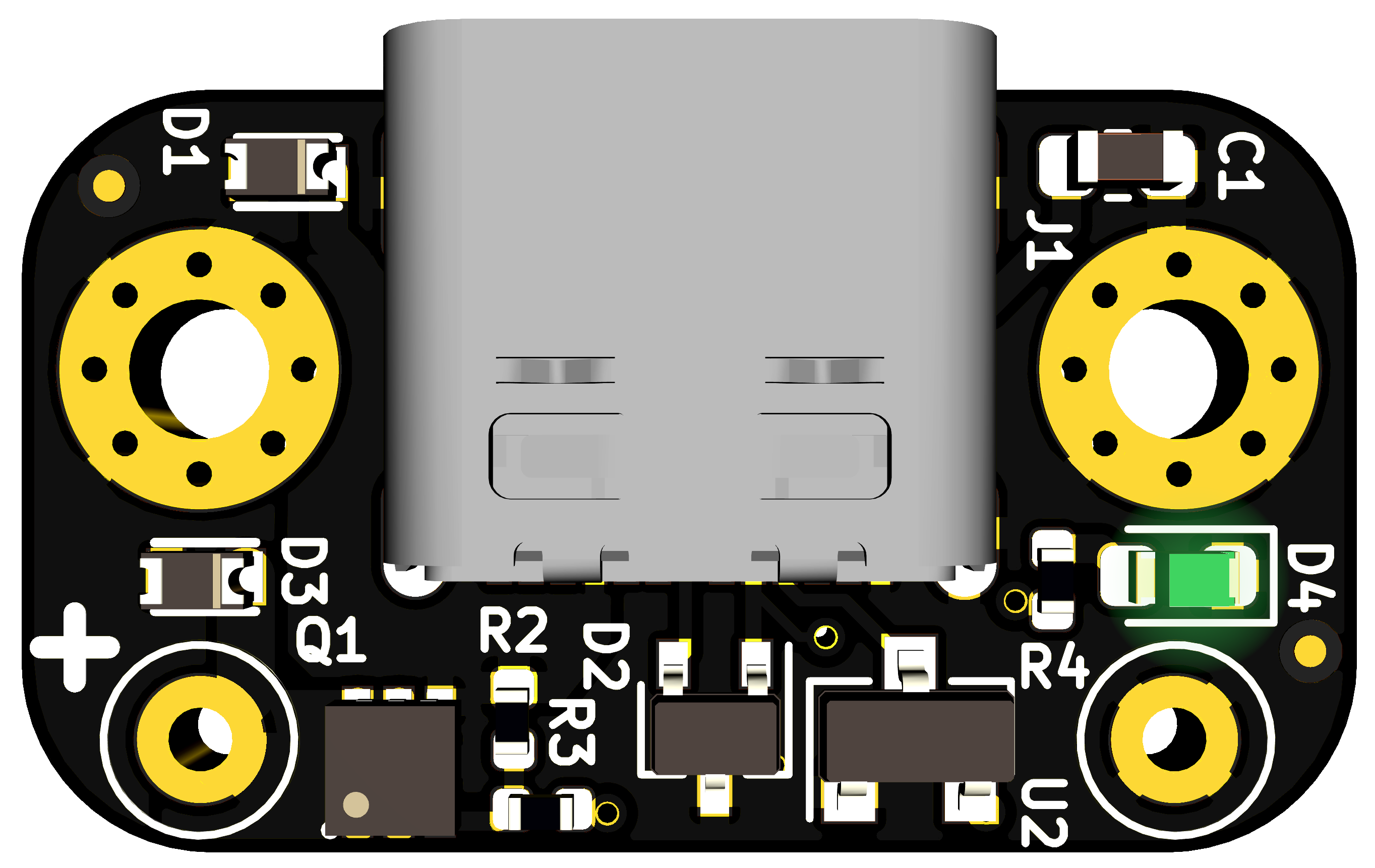
This is a tiny module, measuring 21 mm × 12 mm
Long time ago, I had the idea of setting WiFi passwords for ESP8266 boards using something like morse code as light pulses (and someone actually did this recently). This method would have few advantages over alternative methods, such as wiring up the board to another device or using ESSID station names as password:
- No need for special software to run on a computer/phone which would most likely be limited to certain OSes (or at a high development and maintenance cost to make it ubiquitously available). A simple web page with some javascript code would ensure it would run on just about every “smart” device out there.
- No need for cables to connect to the programmer device.
- More secure as it requires close proximity and unobstructed view of the device.
- Simple to design and implement than more complex protocols and interfaces such as USB, Bluetooth and WiFi.
I thought this was the perfect opportunity for me to try out my idea. It took a bit of thinking to come up with some signal processing methods and further changes to arrive at a fairly robust setup. There is a lot more room for improvement of course.
Speaking of signal processing, I had no prior experience with it. I decided to see how far I could get without turning to literature. I wanted the board to adapt to both, varying light conditions, as well as varying light flash rate, as there was no way to ensure a specific screen refresh rate. Even if there was only one rate right now, I wanted to make the board future proof to some degree.
Architecture
Architecture is a strong word for what makes up fpx. Following are the main components and the reason for picking each:
- STUSB4500: already quite familiar with it and it does the heavy lifting when it comes to talking USB-PD
- ATtiny 816 microcontroller: used to read light pulses and program STUSB4500; another familiar chip I’ve used in the past; it also uses the newer UPDI single wire in-circuit programming and debugging interface which requires less space on the board for pads.
- Phototransistor: very cheap and requires the least number of supporting components (just a resistor) while providing very fast response times (compared to full fledged light sensors with digital interfaces).
The rest are supporting components. As you can see, this is a very simple board.
Detecting levels
First order of business is to turn the analog signal coming from the phototransistor to ones and zeros. To ensure a robust performance in varying light conditions, I knew I had to write an adaptive algorithm that just like human eyes, can tune its thresholds continuously. What I came up initially was:
- take ADC readings and store a rolling window of the last
Nsamples - after each reading, calculate the min and max across this window
- determine the thresholds between the min and max
- store the bit values based on the thresholds for the next process

ADC readings are continously taken 10000 times per second.
This worked fine of course, but N had to be a large number to allow for
reading from slow programmers. And given the small amount of RAM
available on ATtiny 816, I went with time blocks instead of a rolling
window. With time blocks, I only needed to keep track of min and max
values, every N time period, which meant that more time was
needed to adapt to lighting conditions. However less storage was needed
as I was no longer storing ADC samples. As you will see later, this can
be easily catered for by a longer preamble.
I also delegated storing bit values (sort of) to the next layer.
Detecting bits
Because of the requirement to be adaptive to the rate at which data is
received, we can’t simply read the bit values at every t
second. We first need to know what t is. Even if we know
what t is, the onboard clock and that of the sender are not
100% accurate and they can drift. That means that not only do we need
to know what t is, but also when to align our readings such
that we don’t hit close to where the bit transitions are happening.
Up to this point, we know what range of ADC values is considered a bit value of zero and one. Instead of storing every bit value, we can store the length of time between each bit transition. We can now adapt to the length between transitions over a period of time just like we did with light levels in the previous section.
We can store a rolling window of time spans between transitions and calculate min, max and thresholds. We can then denote a bit value of 1 to the longer spans and a bit value of 0 to the shorter ones.

This transformation basically turns absolute timing into relative timing.
Encoding data
Now that we have a stream of bit values, we can start reading data, but
how do we know where to start? The obvious choice is to have a certain
pattern that marks the start of a packet of data and then read
N bits right after it. The next thing to consider is
integrity of data. The obvious choice here is to send along a checksum
of data and check it on the receiving end. It then occurred to me that I
could do without the starting pattern.
After reading each bit, the last N bits would be tested for
a valid packet by calculating the checksum and testing it against the
received data.

OK, not quite. We still need the preamble in order to allow the ADC signal level processor to adapt to the lighting condition.
Performance
I managed to get by, inventing my way through the signal processing part, without googling! This was the most satisfying aspect of this project. The lesson here is that you can get quite far using simple methods. I would like to learn more about signal processing of course, but learning by trial and error has always had a certain sense of wonder for me.
There is one performance issue and that is ambient infrared light negatively affecting reads. The phototransistor I picked is most sensitive to IR light and therefore the board doesn’t work quite well in a sunny room or under tungsten lights. Unfortunately, I couldn’t readily find phototransistors suited for the visible spectrum at the time. I have thought of using IR blocking adhesives and other filtering methods to apply to the board, but haven’t found a solution yet.
The board and all of its supporting code, design files and more are available under an MIT open source license.